HBM Is 16x Wider Than DDR5. AI Chips Still Wait on It
Why AI chips stall on memory, how stacked HBM widens the data path to 2,048 bits, and what Micron and a 2024 paper say about the limits.
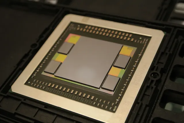
Photo: C. Spille/pcgameshardware.de · CC BY-SA 4.0 · source

The fastest AI chip in the world is useless for the moments it spends waiting for data. That is the problem behind a type of memory most people never see: high-bandwidth memory, or HBM, the stacked chips that sit right next to the processor in AI accelerators.
Micron, one of the companies that make it, describes HBM as built to overcome memory bandwidth limitations. Its pitch is simple: a fast flow of data “keeps processors busy rather than waiting for data.” This article explains what that means, how HBM is built, what the 2026 numbers are, and why even a very wide pipe has not made the problem go away.
The problem: compute grew faster than memory
An AI processor does two jobs. It calculates, and it fetches the numbers to calculate with. A 2024 paper by Amir Gholami and five co-authors, “AI and Memory Wall,” puts figures on how unevenly the two have improved. Over the past 20 years, the authors write, peak server hardware compute has scaled at 3.0x every two years. DRAM bandwidth scaled only 1.6x and interconnect bandwidth 1.4x over the same period.
Compounded for two decades, that gap is large. The paper’s conclusion is that memory, rather than compute, has become the primary bottleneck in AI applications, especially when a trained model is serving answers. It singles out decoder Transformer models, the design behind chatbots that write text one piece at a time, as the case where memory bandwidth can be the dominant limit. In plain terms: such a model keeps going back to its stored numbers, so the speed of that trip matters as much as the speed of the arithmetic.
Two different things are easy to confuse here. Micron’s HBM4 page separates them: capacity decides what data fits in memory, and bandwidth decides how quickly it can be read. HBM is mostly a bandwidth fix.
How HBM is built
Ordinary memory modules sit on a circuit board, some distance from the processor. HBM changes the geometry in two ways, according to Micron.
- It stacks. Micron calls HBM a “3D-stacked” memory in which several DRAM dies are placed on top of each other, on an optional base die. The layers are connected by thousands of through-silicon vias (TSVs), which are tiny vertical channels through the silicon, plus microbumps.
- It sits next to the processor. HBM is integrated into a system-in-package alongside the CPU or GPU via a silicon interposer, which shortens the distance data must travel.
The result is a very wide interface rather than a very fast narrow one. Micron says a single HBM cube has a 1024-bit-wide data interface with 32 independent channels, which it describes as 16 times wider than a standard DDR5 module. That is the origin of this article’s headline number, and the comparison is Micron’s own.
The photo at the top shows the layout on a real chip. It is a 2015 AMD graphics package, described on Wikimedia Commons as holding the GPU, HBM memory and interposer. The large square in the middle is the processor, and four smaller blocks sit directly beside it. It is not a current AI accelerator, but the arrangement is the same idea.
The 2026 numbers: HBM4
The latest generation, HBM4, doubles the interface width. Micron’s HBM4 page describes a 2048-pin bus running at more than 11.0 Gbps per pin and “greater than 2.8 TB/s” of bandwidth per stack. For comparison, the same company lists its previous HBM3E at more than 1.2 TB/s per stack, and puts the HBM4 gain at 2.3 times, based on its own testing and validation.
You can check the headline figure yourself, as our arithmetic rather than a claim from the page: 2,048 pins times 11 gigabits per second is 22,528 gigabits per second, which divided by 8 is about 2,816 gigabytes per second, or roughly 2.8 TB/s. Width times speed is the whole formula, and HBM4 raised the width.
Other details from Micron’s page:
- A 12-high HBM4 stack holds 36 GB, which is the same capacity as the previous generation’s 12-high stack.
- A 16-high, 48 GB version is listed as sampling to customers.
- Micron states a power-efficiency improvement of more than 20% over HBM3E, measured in picojoules per bit at similar speeds.
- The page’s timeline lists an HBM4 volume ramp in 2026.
Micron’s figures are the company’s own, measured against its own earlier products, so they describe one vendor’s parts rather than the whole market.
Why a wider pipe does not end the problem
Notice what HBM4 did to the bottleneck. Per Micron’s numbers, one generation more than doubled bandwidth, 2.3 times. The 2024 paper’s historical figure for DRAM bandwidth is 1.6 times every two years. HBM4 is a big step on that scale, but the paper’s point is about the trend: the demand side, meaning compute and model size, has been growing faster than any memory interface so far.
Heat and cost enter as well. Stacking 12 or 16 dies is demanding. Micron’s FAQ says the vertical design requires higher precision in manufacturing, making HBM one of the more challenging memory products to produce. None of the sources we checked publishes prices or supply, so this article does not estimate them.
The authors of the 2024 paper argue that hardware alone will not close the gap. They call for redesigning model architectures, training methods and deployment strategies, so that models need fewer trips to memory in the first place. That is a research argument, not a settled fact, and it was made before HBM4 existed.
What this means for AI power use
Moving data costs energy as well as time, which is one reason Micron lists energy per bit among HBM4’s headline features. For the wider picture of what AI facilities draw from the grid, see our explainer on AI data-center consumption.
What to take from it
First, HBM is a way to get more bandwidth by going wide and close: stacked dies, a very wide bus, and a seat right next to the processor. Second, the 2.8 TB/s headline is simply 2,048 pins times 11 Gbps, a number worth checking whenever a vendor quotes one. Third, the figures come from one maker’s own pages and a single academic paper, and Micron’s page does not claim that HBM4 ends the memory bottleneck. Whether a given AI chip is held back by memory or by compute depends on the model it runs, which is why the same chip can look quick on one task and idle on another.
What the sources do not yet answer is how much real-world AI speed HBM4 adds across different workloads. Independent benchmarks would be needed for that, and we did not find any in the primary sources used here.